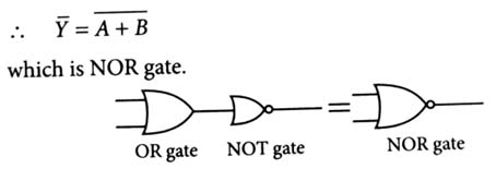
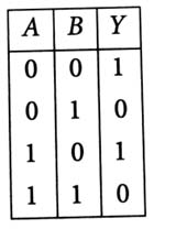
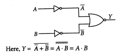
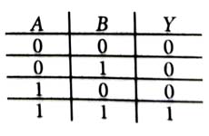
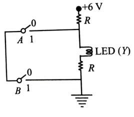
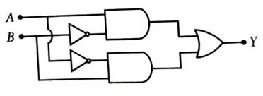
The output (Y) of the given logic implementation is similar to the output of an/a _______ gate. [2025]

OR
NOR
AND
NAND
(2)

The output Y for the inputs A and B of the given logic circuit is [2024]

(3)

When the output of an OR gate is applied as input to a NOT gate, then the combination acts as a [2024]
NAND gate
NOR gate
AND gate
OR gate
(2)
For OR gate, Y = A + B
NOT gate is applied to Y,

So, when output of OR gate is applied as input to a NOT gate, then the combination acts as a NOR gate.
A logic circuit provides the output Y as per the following truth table: [2024]

The expression for the output Y is
(3)
Given truth table:
| A | B | Y |
| 0 | 0 | 1 |
| 0 | 1 | 0 |
| 1 | 0 | 1 |
| 1 | 1 | 0 |
The given truth table is satisfied by, the expression,
The output (Y) of the given logic gate is similar to the output of an/a [2024]

NAND gate
NOR gate
OR gate
AND gate
(4)

So, the output Y represents AND gate.
For the following logic circuit, the truth table is [2023]


(4)

Here, NAND gate is followed by two NOT gates.
By using A = 0, B = 0, we get Y = 0
A = 0, B = 1, Y = 1
A = 1, B = 0, Y = 1
A = 1, B = 1, Y = 1
This corresponds to OR gate.

The truth table for the given logic circuit is [2022]


(3)
Output of the given circuit is

Therefore, the correct truth table corresponding to is
| A | B | C = |
| 0 | 0 | 1 |
| 0 | 1 | 0 |
| 1 | 0 | 1 |
| 1 | 1 | 0 |
For the given circuit, the input digital signals are applied at the terminals A, B and C. What would be the output at the terminal y? [2021]


(3)

Output of combination of logic gates is given as

The output (y) can be represented as above.
For the logic circuit shown, the truth table is [2020]

| A | B | Y |
| 0 | 0 | 0 |
| 0 | 1 | 0 |
| 1 | 0 | 0 |
| 1 | 1 | 1 |
| A | B | Y |
| 0 | 0 | 0 |
| 0 | 1 | 1 |
| 1 | 0 | 1 |
| 1 | 1 | 1 |
| A | B | Y |
| 0 | 0 | 1 |
| 0 | 1 | 1 |
| 1 | 0 | 1 |
| 1 | 1 | 0 |
| A | B | Y |
| 0 | 0 | 1 |
| 0 | 1 | 0 |
| 1 | 0 | 0 |
| 1 | 1 | 0 |
(1)

This AND Gate. So, the truth table is


The correct Boolean operation represented by the circuit diagram drawn is [2019]
NOR
AND
OR
NAND
(4)
LED bulb will light up if switch(s) A or B or both A and B is/are open. Hence it represents a NAND gate.